ASML Unveils Power Breakthrough to Boost Chip Output by Fifty Per Cent
Veldhoven, Tuesday 24 February 2026
By doubling the frequency of molten tin droplets, ASML has achieved a 1,000-watt light source, projected to boost chip production by 50 per cent by 2030 and secure its market dominance against emerging rivals.
A Quantum Leap in Lithography Power
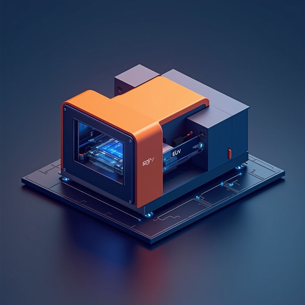
In a decisive move to fortify its command over the semiconductor equipment sector, ASML Holding revealed a pivotal technological advancement on Monday, 23 February 2026 [1][5]. Researchers at the Veldhoven-based company have successfully increased the power of the Extreme Ultraviolet (EUV) light source in their lithography systems to 1,000 watts, a substantial rise from the current standard of 600 watts [2][8]. This development is not merely incremental; it represents a critical evolution in the semiconductor value chain, designed to keep the Dutch giant well ahead of emerging competition from both the United States and China [1]. The breakthrough relies on a sophisticated interplay of physics and engineering, utilising precision optics from German partner Carl Zeiss AG to capture and direct the intensified light for chip printing [2][5].
Engineering the Extreme
The mechanism behind this power surge involves a highly complex manipulation of matter. To generate EUV light with a wavelength of 13.5 nanometres, ASML’s machines fire molten tin droplets through a chamber where they are struck by a high-powered carbon dioxide laser to create plasma [2][5]. The key innovation lies in the frequency and precision of this process: the new technology doubles the number of tin droplets to approximately 100,000 per second [2][5]. Furthermore, the system now employs two smaller laser pulses—rather than the single pulse used in previous generations—to shape these droplets into plasma more effectively [2][8]. Jorge J. Rocca, a professor at Colorado State University, described the achievement of one kilowatt of power as ‘pretty amazing’, noting the immense challenge of mastering the multiple technologies involved [2].
Throughput Gains and Economic Impact
For chip manufacturers such as TSMC and Intel, the primary metric of value is throughput—the speed at which silicon wafers can be processed [1]. Currently, ASML’s machines process approximately 220 wafers per hour [2]. With the implementation of the 1,000-watt light source, the company projects that factories will be able to process 330 wafers per hour by the end of the decade [2][7]. This represents a production increase of 50 per cent. Teun van Gogh, Executive Vice President for the NXE line at ASML, emphasised the economic rationale, stating that the company aims to ensure customers can continue using EUV technology at a ‘much lower cost’ [2][5].
Fortifying the Competitive Moat
This technological leap serves as a strategic bulwark against a backdrop of intensifying geopolitical friction and commercial rivalry. While ASML currently stands as the sole global manufacturer of commercial EUV machines, the United States government has restricted shipments to China, prompting Beijing to accelerate its own development efforts [1][8]. Simultaneously, American startups such as Substrate and xLight are actively developing competing technologies [1]. However, ASML’s lead technologist Michael Purvis dismissed the notion that the new power level is experimental, asserting it is ‘not a parlor trick’ but a robust system capable of operating under customer requirements [1][2]. Looking ahead, the company sees a clear path to further increasing the source power to 1,500 watts, with potential to reach 2,000 watts in the future [2][5].
Sources & Ecosystem Partners
- www.reuters.com
- www.techzine.eu
- www.techzine.nl
- www.bnr.nl
- www.iex.nl
- www.hln.be
- www.technologyinsider.nl
- nl.marketscreener.com