
Dutch Startup Raises €20.7 Million to Fix the Electronics Industry's Biggest Manufacturing Flaw
Eindhoven, Sunday 20 September 2026
Eindhoven-based Keiron Printing Technologies has secured €20.7 million to scale laser technology that resolves solder defects, which currently cause 70 per cent of all electronics manufacturing failures.
Resolving a €600 Billion Bottleneck
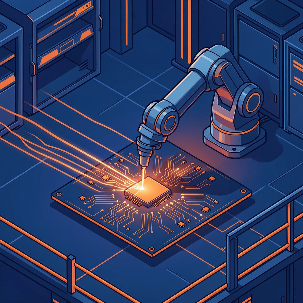
In the global electronics assembly market, valued at an estimated €600 billion, traditional manufacturing processes have long struggled with precision [2]. Solder paste printing issues are historically responsible for over 70 per cent of all defects in electronics manufacturing [2]. Eindhoven-based Keiron Printing Technologies aims to eliminate these systemic failures entirely through its proprietary laser-assisted deposition technology [1][2]. The company’s flagship HF2 LiFT printer replaces traditional stencil printers, jet printers, and inspection systems with a single digital, non-contact platform, simplifying a notoriously complex assembly chain [2].
Dramatic Yield Improvements
By removing the mechanical limitations of stencils and jetting, Keiron’s technology delivers dramatic improvements in production efficiency [1][2]. The non-contact platform increases first-pass yield from approximately 60 per cent to above 95 per cent, whilst simultaneously doubling production uptime [2]. Furthermore, the system accelerates programming times by 10 times, offering unprecedented flexibility for high-tech systems and materials (HTSM) manufacturers who require rapid prototyping and high-mix, low-volume production runs [2][GPT].
Powering Next-Generation AI and Defence Hardware
This level of precision is becoming mandatory as the industry transitions to next-generation hardware [2][GPT]. Modern artificial intelligence hardware, advanced robotics, quantum computing components, and dual-use defence systems demand circuitry with extreme interconnect density [GPT]. Conventional printing methods fail when components feature up to 10,000 interconnects, a threshold that Keiron’s laser-assisted deposition platform is specifically designed to surpass [1][2]. By enabling the precise placement of solder paste at this microscopic scale, the technology secures the assembly of highly complex, high-performance physical systems [1][2].
From Laboratory Innovation to Industrial Scale
Keiron’s journey represents a successful transition within the Dutch deeptech ecosystem, moving from laboratory research to industrial-scale manufacturing [1]. The company evolved existing laboratory-grade laser technology by integrating its own proprietary optics, measurement systems, and software [1]. Prior to this Series A round, the firm received early-stage public support via an Innovation Credit (Innovatiekrediet) from the Netherlands Enterprise Agency (RVO) [1]. This blend of early public backing and subsequent private venture capital has allowed the company to mature its hardware for commercial deployment [1].
Strategic Backing for Commercial Scaling
The €20.7 million Series A funding round represents a major milestone, with Dutch impact investor Invest-NL leading the commitment with €6.9 million [1], representing 33.333 per cent of the total round. Invest-NL co-led the round alongside DeepTechXL and Waves Capital, with further participation from Ramphastos Investments, TNO Ventures, ATUM Ventures, and Cottonwood Technology Fund [1][2]. Maaike Vranckaerts, investment manager at Invest-NL, highlighted that Keiron’s proposition holds the potential for true breakthrough innovation, fully developed within the Dutch high-tech ecosystem [1]. Keiron plans to use the capital to validate the technology with customers, scale its initial systems, establish a dedicated service organisation, and develop the next generation of its platform [1].